Home > NEWS > Surface Measurement Methods for Thin-Plane Parallel Optics
Measuring the surfaces of thin, parallel optics can be challenging. When optics are less than a few millimeters thick, their front and back surfaces are so close together that it is difficult for standard interferometry to tell them apart. Fortunately, the right metrology equipment makes it possible to distinguish the surfaces and characterize the quality of both in a single measurement, even if they are less than a millimeter thick.
Thin Is In
Thin, planar optics are in increased demand these days, typically in semiconductor and consumer electronics applications. As manufacturers work to put more capabilities into their devices, they are also pressured to reduce the thickness and mass. Manufacturers introducing flexible smartphones, for example, require thin, bendable displays.
Optics manufacturers need to ensure that the surface form of thin glass is flat and free of material deformities as variations in the substrate and its surface characteristics can cause visible distortions in the display.
Commercial solutions exist for the metrology of plane parallel optics, such as wavelength shifting and low-coherence interferometry. A more advanced wavelength shifting technique is Fourier-transform phase-shifting interferometry (FTPSI), which enables easy characterization of the front and back surface, optical thickness variation, and material homogeneity of thin plane parallel glass.
Hard To Separate
Traditional mechanical phase shifting interferometry (PSI) can’t distinguish the front surface of a thin, parallel optic from the back surface because the two surfaces are so physically close together. PSI works by passing a light beam through an ideal reference optic, called a transmission flat (TF), to the part under test. Phase shifting is achieved with a calibrated mechanical motion of the TF. When properly aligned, the TF and the part under test create an interference pattern, recorded as an interferogram. The metrology software analyzes the height variations produced by the phase shifts and reconstructs the surface wavefront, which represents the difference in height between the TF and the test part.
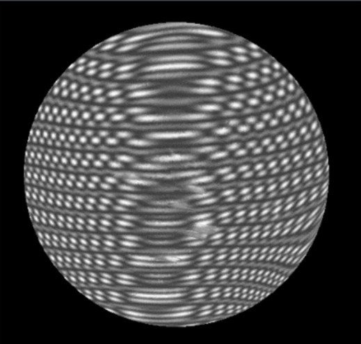
In the case where a thin, parallel part is being measured, a second reflection is returned to the interferometer from the back surface. This results in multiple, overlapping interferograms with a complex fringe pattern that PSI cannot accurately analyze. (See image 1.)

Image 1: Complex fringe pattern caused by multiple surface reflections
Methods have been developed to overcome the fundamental limitations of measuring thin parallel parts with PSI, such as coating the back surface with materials that extinguish its reflection. Applying black paint, coloring with a dark marker, or spreading petroleum jelly on the surface takes time and adds additional, undesirable steps to the metrology process. Operators also run the risk of damaging or distorting a thin part.
FTPSI acquisition does not require manipulation of the back surface. It actually uses the back surface reflection to gain more information about the part in a single measurement. Instead of relying on mechanical motion within the measurement cavity, FTPSI depends on modulation of the wavelength of the laser to create the measurement. Each cavity in the optical path in an FTPSI acquisition produces a unique interference frequency that defines its cavity length, enabling a clear delineation and accurate characterization of each surface.
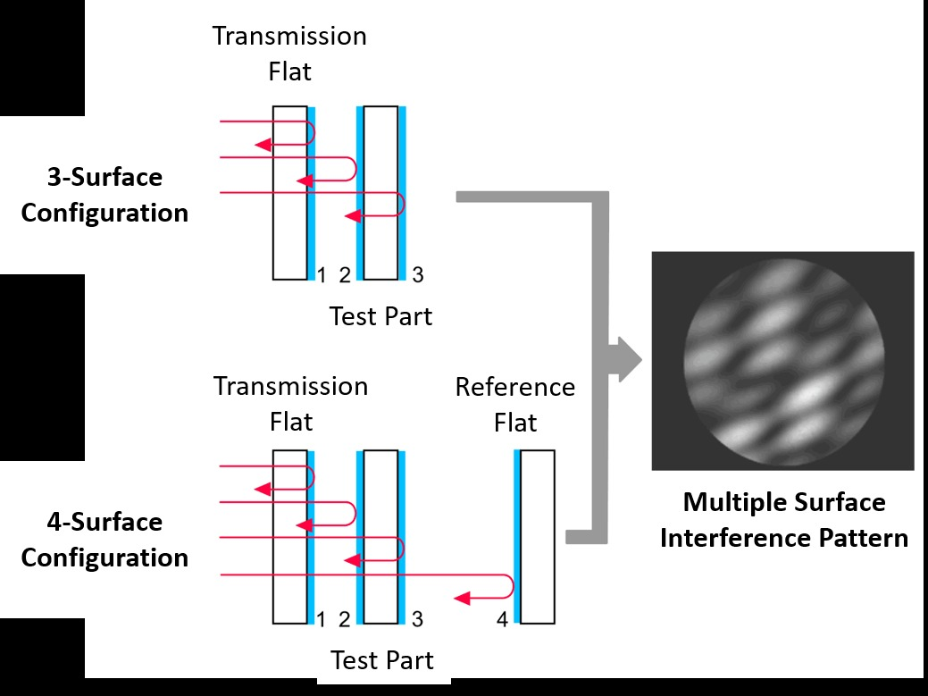
The algorithms, then, can analyze multiple wavefronts and characterize the form of each surface independently. The simplest FTPSI measurement is a three-surface configuration that consists of the TF (surface #1) and the test part (surfaces #2 and #3). (See image 2.) In this configuration, the back surface result will include material non-uniformities. For higher accuracy measurements of the back surface, a four-surface configuration can be used by placing a reference flat (RF, surface #4) behind the test optic. In this configuration, the form of surface #3 is compared to the known RF without the contribution of the material in the part.

Image 2: Example of a 3-surface and 4-surface configuration
The 20th anniversary of Oplens
Dec. 29, 2025SPIE Photonics West Exhibition: 20 – 22 January 2026
Dec. 19, 2025